- 您现在的位置:买卖IC网 > Sheet目录1994 > DS1678S/T&R (Maxim Integrated Products)IC RECORDER REALTIME EVENT 8SOIC
DS1678 Real-Time Event Recorder
4 of 25
Note 1:
Limits at -40
C are guaranteed by design and not production tested.
Note 2:
All voltages referenced to ground.
Note 3:
After this period, the first clock pulse is generated.
Note 4:
A device must initially provide a hold time of at least 300ns for the SDA signal to bridge the undefined region of the falling edge
of SCL. The maximum tHD:DAT need only be met if the device does not stretch the LOW period (tLOW) of the SCL signal.
Note 5:
A fast-mode device can be used in a standard-mode system, but the requirement tSU:DAT > 250ns must then be met. This is
automatically the case if the device does not stretch the LOW period of the SCL signal. If such a device does stretch the LOW
period of the SCL signal, it must output the next data bit to the SDA line tR(MAX) + tSU:DAT = 1000 + 250 = 1250ns before the SCL
line is released.
Note 6:
CB—Total capacitance of one bus line in pF.
Note 7:
tR and tF are measured with a 1.7k pullup resistor, 200pF pullup capacitor, 1.7k pulldown resistor, and 5pF
pulldown capacitor.
I
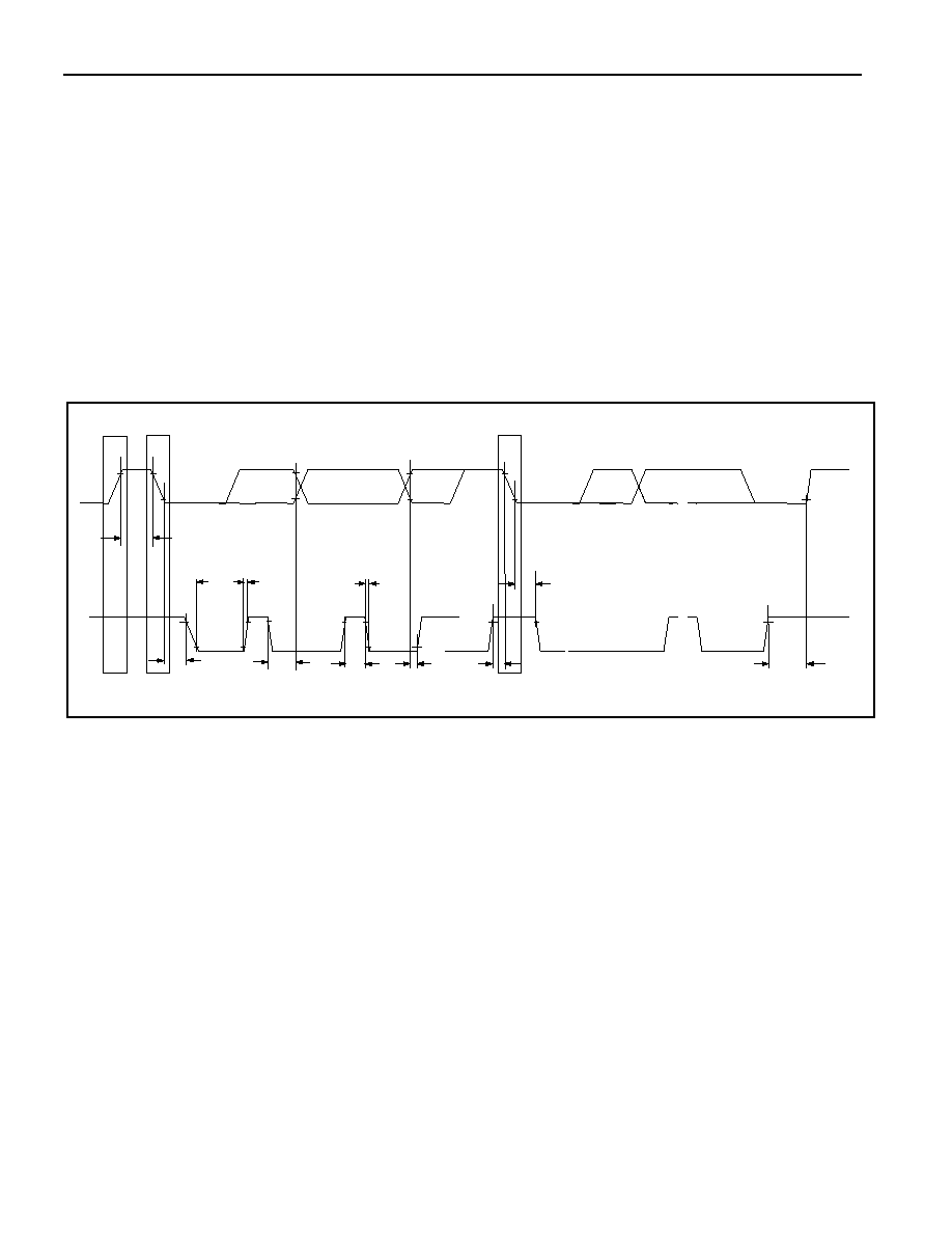
2C COMMUNICATION TIMING DIAGRAM
SU:STO
t
HD:STA
t
t SU:STA
SU:DAT
t
tHIGH
R
t
tLOW
tHD:STA
SCL
START
SDA
STOP
tBUF
tF
REPEATED
START
tHD:DAT
发布紧急采购,3分钟左右您将得到回复。
相关PDF资料
DS1682S
IC TIMEKEEPER ALARM ELAPSE 8SOIC
DS1683S+T&R
IC REAL TIME EVENT REC 8SOIC
DS1685EN-5/T&R
IC RTC 5V 64BIT Y2K IND 24TSSOP
DS1688S+
IC RTC W/NV RAM CTRL 28-SOIC
DS1689SN+T&R
IC RTC SER NV RAM CTRL IN 28SOIC
DS17285S-3NT
IC RTC 3V 2K NV RAM 24-SOIC
DS1742-100IND
IC RTC RAM Y2K 5V 100NS 24-EDIP
DS1743P-70+
IC RTC RAM Y2K 5V 70NS 34-PCM
相关代理商/技术参数
DS1678S+
功能描述:实时时钟 Real-Time Event Recorder RoHS:否 制造商:Microchip Technology 功能:Clock, Calendar. Alarm RTC 总线接口:I2C 日期格式:DW:DM:M:Y 时间格式:HH:MM:SS RTC 存储容量:64 B 电源电压-最大:5.5 V 电源电压-最小:1.8 V 最大工作温度:+ 85 C 最小工作温度: 安装风格:Through Hole 封装 / 箱体:PDIP-8 封装:Tube
DS1678S+T&R
制造商:Maxim Integrated Products 功能描述:REAL TIME CLOCK SERL 32BYTE 8SOIC - Tape and Reel 制造商:Maxim Integrated Products 功能描述:IC REAL TIME EVENT REC 8-SOIC 制造商:Maxim Integrated Products 功能描述:Real Time Clock Real-Time Event Recorder
DS1678S+T&R
功能描述:实时时钟 Real-Time Event Recorder RoHS:否 制造商:Microchip Technology 功能:Clock, Calendar. Alarm RTC 总线接口:I2C 日期格式:DW:DM:M:Y 时间格式:HH:MM:SS RTC 存储容量:64 B 电源电压-最大:5.5 V 电源电压-最小:1.8 V 最大工作温度:+ 85 C 最小工作温度: 安装风格:Through Hole 封装 / 箱体:PDIP-8 封装:Tube
DS1678SR
制造商:MAXIM 制造商全称:Maxim Integrated Products 功能描述:Real-Time Event Recorder
DS1678ST
制造商:MAXIM 制造商全称:Maxim Integrated Products 功能描述:Real-Time Event Recorder
DS1679
制造商:未知厂家 制造商全称:未知厂家 功能描述:
DS1679B
制造商:Maxim from Components Direct 功能描述:THE MAXIM DS1679B IS A LOW-SIDE MOSFET DRIVER. - Rail/Tube 制造商:Maxim 功能描述:The Maxim DS1679B is a Low-Side MOSFET Driver.
DS1679BS
制造商:Rochester Electronics LLC 功能描述: 制造商:Maxim Integrated Products 功能描述: